- 您现在的位置:买卖IC网 > Sheet目录2007 > MAX1098CEAE+ (Maxim Integrated Products)IC ADC 10BIT SERIAL 16-SSOP
MAX1098/MAX1099
10-Bit Serial-Output Temperature Sensors
with 5-Channel ADC
2
_______________________________________________________________________________________
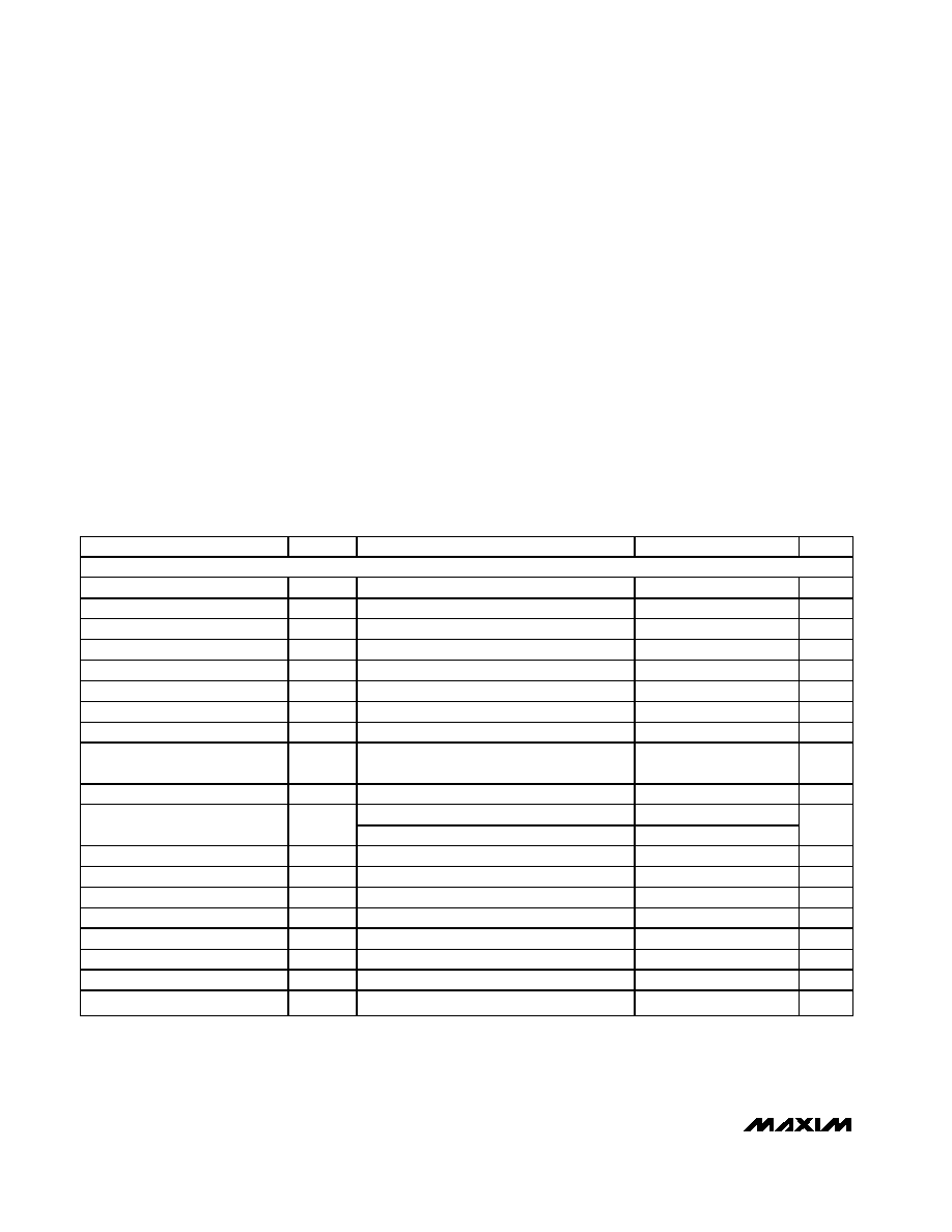
ABSOLUTE MAXIMUM RATINGS
ELECTRICAL CHARACTERISTICS
(VDD = +4.75V to +5.25V (MAX1098), VDD = +2.7V to +3.6V (MAX1099), external reference, VREF = +2.5V (MAX1098), VREF = +1.2V
(MAX1099), fSCLK = 2.5MHz, TA = TMIN to TMAX, unless otherwise noted. Typical values are at TA = +25°C.)
Stresses beyond those listed under “Absolute Maximum Ratings” may cause permanent damage to the device. These are stress ratings only, and functional
operation of the device at these or any other conditions beyond those indicated in the operational sections of the specifications is not implied. Exposure to
absolute maximum rating conditions for extended periods may affect device reliability.
VDD to GND.……………………………………………-0.3V to +6V
SHO to GND ................................................-0.3V to (VDD +0.3V)
Analog Inputs to GND
(AIN0–AIN5, REF)...................................-0.3V to (VDD +0.3V)
Digital Inputs to GND (DIN, SCLK, CS).......-0.3V to (VDD +0.3V)
Digital Outputs to GND (DOUT, SSTRB) .....-0.3V to (VDD +0.3V)
Digital Output Sink Current ..…………………………………25mA
Maximum Current into Any Pin……………………………….50mA
Continuous Power Dissipation (TA = +70°C)
16-Pin SSOP (derate 8.00mW/°C above +70°C) ........667mW
Operating Temperature Range
MAX109_ _EAE ...............................................-40°C to +85°C
Junction Temperature....……………………………………+150°C
Storage Temperature Range .............................-65°C to +150°C
Lead Temperature (soldering, 10s) .................................+300°C
PARAMETER
SYMBOL
CONDITIONS
MIN
TYP
MAX
UNITS
DC ACCURACY (Note 1)
Resolution
RES
10
Bits
Relative Accuracy (Note 2)
INL
±1
LSB
Differential Nonlinearity
DNL
±1
LSB
Offset Error
Inputs AIN0
AIN5
±1
LSB
Offset Temperature Coefficient
±10
V/°C
Gain Error
Inputs AIN0
AIN5, offset nulled
±1
LSB
VDD/4 Absolute Error
±1
LSB
Gain Temperature Coefficient
±2
ppm/
°C
Channel-to-Channel Offset
Matching
±0.25
LSB
CONVERSION RATE
Voltage measurement
1.1
Conversion Time (Note 3)
tCONV
Temperature measurement
2.2
ms
Track/Hold Acquisition Time
tACQ
16
s
Aperture Delay
tAPR
30
ns
Internal Clock Frequency
fCLK
57.6
62.3
65.5
kHz
ANALOG INPUTS (AIN0
AIN5)
Input Voltage Range (Note 4)
Measurement with respect to IN-, Figure 1
-2VREF
+2VREF
V
Common-Mode Range
0VDD
V
Input Current (Note 5)
0.1
5
A
Input Capacitance
16
pF
发布紧急采购,3分钟左右您将得到回复。
相关PDF资料
MAX11040GUU+T
IC ADC 24BIT 4CH 38-TSSOP
MAX11046ECB+T
IC ADC 16BIT PAR 250KSPS 64TQFP
MAX11046ETN+T
ADC 16BIT SAMPLING 8CH 56-TQFN
MAX11049ECB+
IC ADC 16BIT PAR 250KSPS 64TQFP
MAX1104EUA+
IC CODEC 8BIT 8-UMAX
MAX11100EUB+
IC ADC 16BIT SRL 200KSPS 10UMAX
MAX11101EUB+
IC ADC 14BIT SRL 200KSPS 10UMAX
MAX11102AUB+
IC ADC 12BIT SPI/SRL 10UMAX-EP
相关代理商/技术参数
MAX1098CEAE+T
功能描述:板上安装温度传感器 10Bit SerialOut Temp Sensor w/5Ch ADC RoHS:否 制造商:Omron Electronics 输出类型:Digital 配置: 准确性:+/- 1.5 C, +/- 3 C 温度阈值: 数字输出 - 总线接口:2-Wire, I2C, SMBus 电源电压-最大:5.5 V 电源电压-最小:4.5 V 最大工作温度:+ 50 C 最小工作温度:0 C 关闭: 安装风格: 封装 / 箱体: 设备功能:Temperature and Humidity Sensor
MAX1098CEAE+W
制造商:Maxim Integrated Products 功能描述:TEMP SENSOR DGTL SERL 16SSOP - Rail/Tube
MAX1098CEAE-T
功能描述:板上安装温度传感器 RoHS:否 制造商:Omron Electronics 输出类型:Digital 配置: 准确性:+/- 1.5 C, +/- 3 C 温度阈值: 数字输出 - 总线接口:2-Wire, I2C, SMBus 电源电压-最大:5.5 V 电源电压-最小:4.5 V 最大工作温度:+ 50 C 最小工作温度:0 C 关闭: 安装风格: 封装 / 箱体: 设备功能:Temperature and Humidity Sensor
MAX1098-MAX1099
制造商:MAXIM 制造商全称:Maxim Integrated Products 功能描述:10-Bit Serial-Output Temperature Sensors with 5-Channel ADC
MAX1099
制造商:MAXIM 制造商全称:Maxim Integrated Products 功能描述:10-Bit Serial-Output Temperature Sensors with 5-Channel ADC
MAX1099AEAE
功能描述:板上安装温度传感器 RoHS:否 制造商:Omron Electronics 输出类型:Digital 配置: 准确性:+/- 1.5 C, +/- 3 C 温度阈值: 数字输出 - 总线接口:2-Wire, I2C, SMBus 电源电压-最大:5.5 V 电源电压-最小:4.5 V 最大工作温度:+ 50 C 最小工作温度:0 C 关闭: 安装风格: 封装 / 箱体: 设备功能:Temperature and Humidity Sensor
MAX1099AEAE+
功能描述:板上安装温度传感器 RoHS:否 制造商:Omron Electronics 输出类型:Digital 配置: 准确性:+/- 1.5 C, +/- 3 C 温度阈值: 数字输出 - 总线接口:2-Wire, I2C, SMBus 电源电压-最大:5.5 V 电源电压-最小:4.5 V 最大工作温度:+ 50 C 最小工作温度:0 C 关闭: 安装风格: 封装 / 箱体: 设备功能:Temperature and Humidity Sensor
MAX1099AEAE+T
功能描述:板上安装温度传感器 RoHS:否 制造商:Omron Electronics 输出类型:Digital 配置: 准确性:+/- 1.5 C, +/- 3 C 温度阈值: 数字输出 - 总线接口:2-Wire, I2C, SMBus 电源电压-最大:5.5 V 电源电压-最小:4.5 V 最大工作温度:+ 50 C 最小工作温度:0 C 关闭: 安装风格: 封装 / 箱体: 设备功能:Temperature and Humidity Sensor